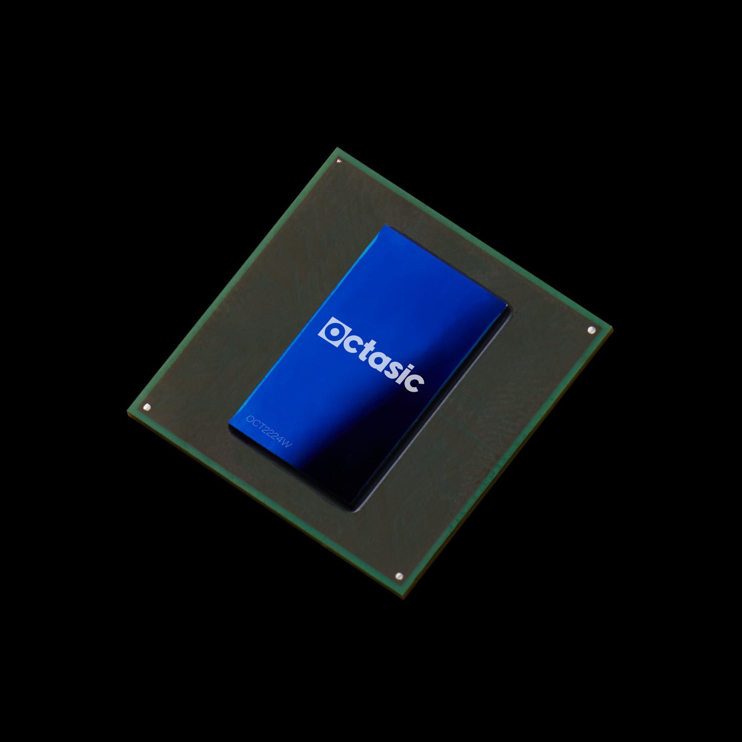
OCT2224W
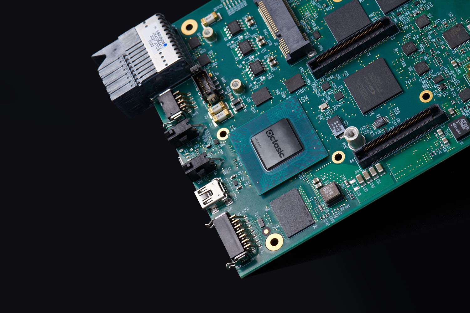
The OCT2224W is a System-on-Chip (SoC) device optimized for LTE, HSPA and GSM baseband processing, with an impressive power-efficiency that consumes less than 5 watts while serving 64 users within a range of 20 km in HSPA. The OCT2224W is highly integrated, and includes high-speed network interfaces as well as on-chip RF ports making it ideal for cost efficient small cell designs.
Tactical Communications
Industrial IoT
Custom Private Networks
The OCT2224W is composed of 24 Opus2 DSP Cores. The DMA subsystem provides a high‐bandwidth interconnect between the cores, peripherals, and external memory.
The OCT2224W includes up to six satellites, each of which is composed of four Opus2 DSP Cores and its own local bus and DMA. Data transfers can be local to the satellite or global.
Octasic DSP Architecture


Specifications
Direct Memory Access (DMA)
Flexible TDM interface
Three parallel interface (PIF) ports
PIF can be adapted to standard video capture and display interfaces such as ITU‐R BT.656 / BT.1120.
484-pin Ball Grid Array (BGA) package, 1.0mm pitch; 4W typical power consumption
Related products